
Announcing Invisix
By Clara Ricard

Building a modern chip is like building a skyscraper at the nanoscale. Before you add the next layer, you have to know the last one developed correctly. But the chips that train and run AI grow more three-dimensional with every generation, and the metrology tools that got the industry here have run out of optical resolution.
That blind spot is one of the most expensive problems in semiconductor manufacturing. When you can’t measure precisely, fabs run lower yields and new nodes take longer to ramp. Manufacturing failures in those layers become harder to catch in realtime, wasting the fab’s time, space, and fabrication power. The existing solutions are slow and destructive, restricting them to off-line use. In a market where being first to a node decides who wins, and a single point on yield can be worth billions, that gap is critical.
Invisix changes that. The company has built an inline metrology system that measures the most complex 3D structures that sit inside advanced chips without destroying them, in real time, at the throughput a high-volume fab actually needs. This means that advanced fabs can see what they’re building while they’re still building it.
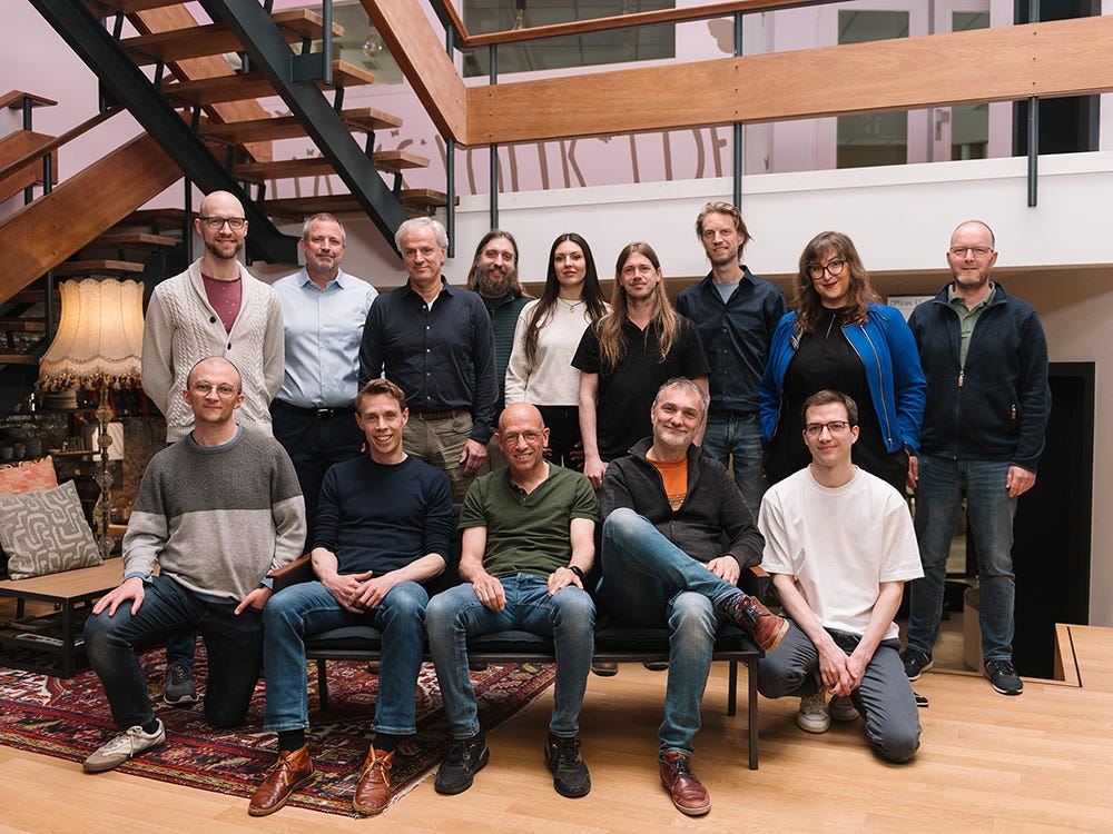
The team
The team is what convinced us. Invisix was founded by two physics PhDs, CEO Christina Porter and CTO Sietse van der Post, who between them spent 20 years on this technology, in academia and at ASML - the Dutch company no chip is made without. They’ve brought a number of its veterans with them, alongside senior operators like COO Roald Dogge, who previously led a similar role at the major chip contract manufacturer NTS. The company’s research stems from a long-standing collaboration with Professor Anne L’Huillier of Lund University, who was awarded the Nobel Prize for her foundational work on this space.
The progress
What’s rare is how far along they already are. In January 2026, they signed a sole license with ASML covering 100+ patents. They’ve proven it works through demonstrations with Intel and imec, as well as a number of others. Its 300mm testbench now sits in a new cleanroom in Eindhoven, where customer demonstrations run continuously alongside the build of the first system designed to ship into a fab.
Looking ahead
It’s especially exciting to make our first investment in Eindhoven, home to ASML and therefore one of the deepest pools of semiconductor manufacturing talent anywhere. Advanced fabs are among the most resource-hungry factories on earth, and catching a fault in real time - without scrapping the wafer to find it - means higher yields, and less wasted energy and material for every chip that ships. We’re proud to back Christina, Sietse and the team as they build one of the machines the next decades of computing depend on.